

Protective Films for Wafer Dicing and Semiconductor Substrates
Sono-Tek ultrasonic coating systems deposit high-quality protective films for wafer dicing, die-cutting, and semiconductor substrate preparation. These thin polymer-based layers protect sensitive surfaces from abrasion, contamination, and damage throughout singulation and handling in clean room environments.
Our programmable ultrasonic platforms precisely deposit durable protective films prior to dicing, helping manufacturers maintain surface integrity and improve downstream yield.
Ultrasonic Precision for Protective Films Prior to Dicing
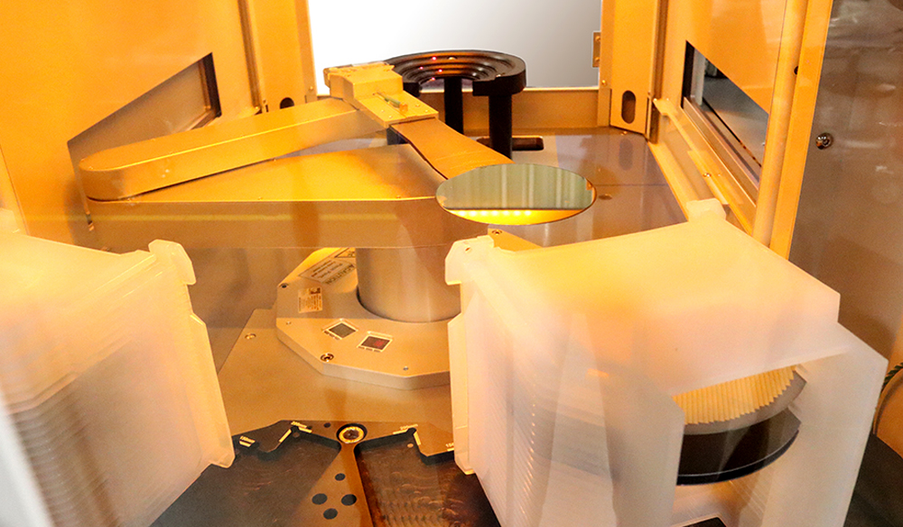
Ultrasonic spray deposition produces a soft, finely controlled mist that forms smooth, uniform polymer coatings across wafers and semiconductor substrates. This enables consistent protective films that support cleaner die-cutting and reduced particle generation.
By adjusting droplet size, spray passes, flow rate, and film thickness, manufacturers can fine-tune:
- Polymer film thickness
- Surface durability and abrasion resistance
- Coating morphology
- Solvent-based or water-based formulations
- Uniform protection across full wafer substrates
These protective films minimize chipping, cracking, and contamination during wafer dicing operations.
Applications for Semiconductor Protective Coatings
Sono-Tek systems support thin protective film deposition for:
- Wafer dicing and singulation
- Die-cutting processes
- Temporary protective polymer coatings
- Back-side and front-side surface protection
- Clean room substrate handling
- Solvent-based temporary films prior to lamination
These coatings help protect high-value semiconductor materials while supporting high throughput manufacturing.
Benefits of Sono-Tek Ultrasonic Protective Film Coating
- Highly uniform protective coatings across full wafer substrates
- Reduced contamination and particle generation during dicing
- Durable, abrasion-resistant polymer layers
- Compatible with solvent-based and water-based chemistries
- Excellent surface protection with minimal material use
- Stable, non-clogging ultrasonic atomization
- Scalable for R&D, pilot, and production environments
- Precision deposition suited for semiconductor clean room workflows
System Options for Protective Film and Surface Protection Coating
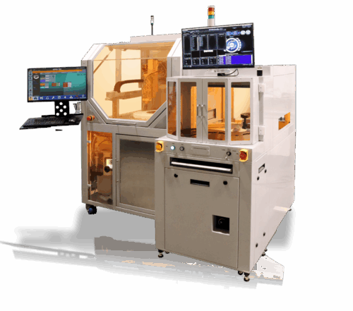
SPT200 – Standalone Ultrasonic Coating System
The SPT200 is a fully enclosed ultrasonic coating platform designed for high-precision semiconductor processes including protective coatings and deep well topographies. Features include high-uniformity heated vacuum chuck, syringe pump with auto-refill, 2-position nozzle rotation, and ISO Class 5 HEPA-filtered enclosure.
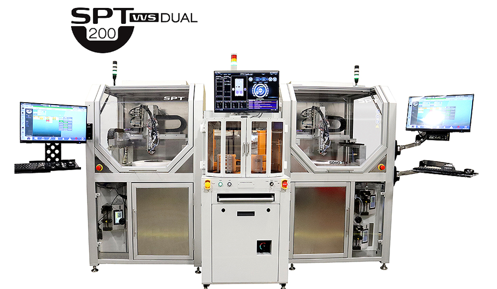
SPT200WS – Automated Wafer Handling Ultrasonic Coating System
The SPT200WS adds fully automated wafer handling for 100–300 mm wafers, with cassette loading, pre-alignment, wafer exhaust, and SEMI-compliant automation. Ideal for higher throughput protective film and photoresist-related processes.
Process Development and Support
Sono-Tek’s Applications Engineering team assists with process development, polymer compatibility, film thickness targeting, coating morphology, and parameter optimization. We help customers achieve consistent, high-quality protective films prior to dicing in both R&D and production environments.
Contact Sono-Tek for Protective Film Coating Solutions – discuss your application or request technical support for selecting a Protective Coating Machine, developing Protective Films for Dicing, or establishing Protective Films Prior to Dicing for semiconductor substrates.