
Photoresist Deposition onto Unconventional Substrates for Microelectronics Manufacturing
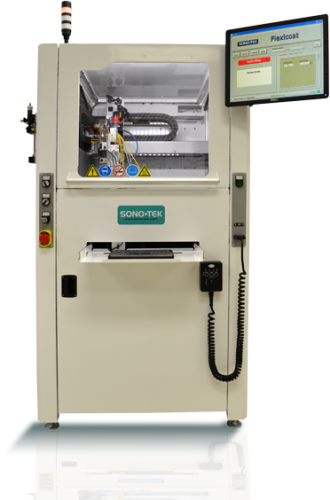
When large, curved, or unconventional substrates make spin coating impractical, Sono-Tek ultrasonic spray coating systems deliver highly uniform, conformal photoresist layers across full surfaces and features. This enables precise photolithography and lithography steps for advanced optical, electronic, semiconductor, and biomedical devices—without pooling, streaking, or excessive edge bead. Ultrasonic spray coating also supports controlled film thickness and reliable adhesion while allowing flexibility in photoresist solvent blends to tune wetting and drying behavior.
Large Optics and Display Panels
For flat panel displays, large lenses, diffractive and anti-reflective optical elements, and other freeform optical components, photoresist coating on flat panels using ultrasonic spray deposition provides complete, edge-controlled coverage. Even on curved or non-planar surfaces, photoresist films remain uniform in thickness after soft bake—ideal for creating AR/VR optics, diffractive structures, and high-resolution photolithography patterns.
Microfluidic and Biosensor Substrates
In microfluidic, biosensor, and lab-on-a-chip manufacturing, spray-applied photoresist adheres well to glass, polymer (PMMA, COC, PDMS), and hybrid surfaces. Controlled droplet atomization produces smooth, solvent-compatible thin films with high pattern fidelity, reducing material use while maintaining consistent dielectric or polymer layer thickness.
Metal and Conductive Surfaces
Photoresist can be deposited directly on metal substrates such as gold, platinum, copper, aluminum, and stainless steel for applications including electrochemical biosensors, MEMS, and microwave/RF circuits. Ultrasonic spraying ensures uniform coverage even on reflective, low-wettability metals and allows fine thickness control for accurate pattern definition along features and sidewalls.
Flexible and Roll-to-Roll Electronics
In flexible electronics, organic thin-film transistors (OTFTs), and flexible solar cells, ultrasonic spray enables solvent-efficient, low-temperature coating compatible with continuous roll-to-roll processing. High transfer efficiency and closed-loop process control minimize chemistry use while maintaining coating precision at scale.
Specialty Polymer and Dielectric Patterning
For photonic crystals, polymer MEMS, metamaterials, and waveguides, spray-deposited photoresist provides conformal masking and templating over micro- and nano-structured surfaces. The process supports a wide range of positive, negative, and UV-curable resist chemistries.
Technical Advantages
- Uniform and conformal coverage across large or curved substrates
- Substantial edge-bead reduction for improved lithography resolution
- Closed-loop thickness control and process repeatability
- Compatible with diverse substrates: glass, polymers, PDMS, metals, flexible films
- High material transfer efficiency, reducing resist and solvent waste
- Scalable for both batch and roll-to-roll production environments
Explore Photoresist Coating for Wafers
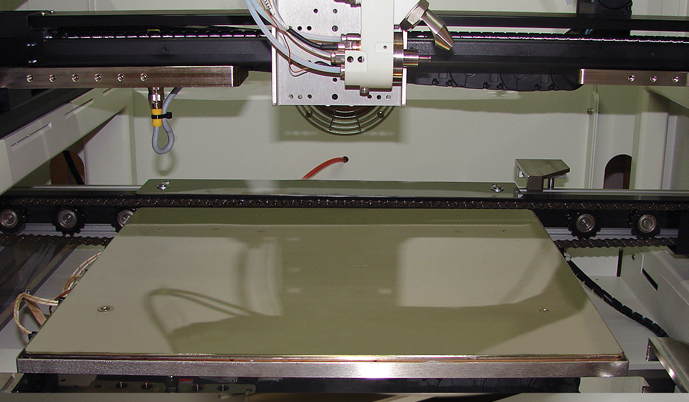
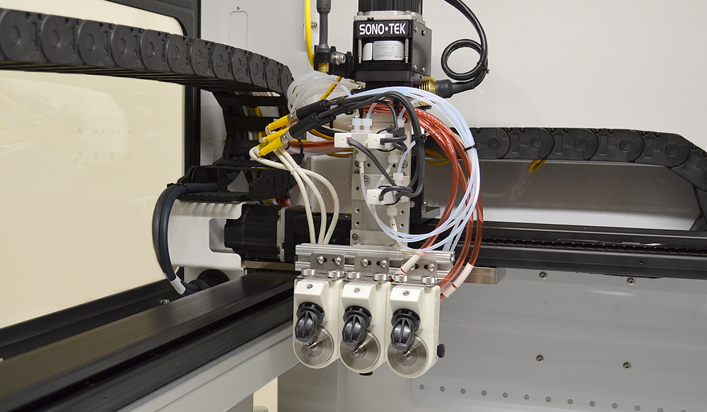
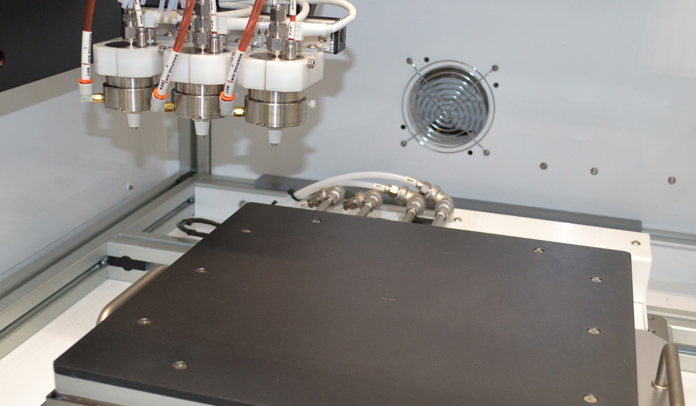
The heart of all Sono-Tek spray systems is our patented ultrasonic spray nozzle, which uses high frequency sound vibrations to produce a soft mist of mathematically defined droplets. This eliminates clogging, since no pressure is used to produce the spray, and the droplets have a very narrow drop distribution size, further contributing to uniformity of the layer deposited. Read more about how our ultrasonic nozzles work.
Read a technical article describing photoresist film coverage improvement using ultrasonic spray technology:photoresist film coverage improvement using ultrasonic spray technology.
If your application involves semiconductor or MEMS wafer processing, visit our dedicated page:
Photoresist Coating onto Semiconductor Wafers