
Sono-Tek’s ultrasonic coating systems enable precision thin-film deposition for advanced microelectronic devices and electronic components. From thin-film photoresist and conductive polymers to EMI shielding and flux films for advanced packaging, our platforms deliver uniform coatings with excellent material efficiency, adhesion, and repeatability. Using low-velocity ultrasonic atomization, we provide controllable, solvent-compatible coating solutions that achieve consistent film quality across complex substrates while minimizing waste.
Our systems support development through full-scale production in applications including photoresist on microelectronics, CNTs/nanowires/conductive inks and nanomaterials, EMI shielding, sensors, MicroLED and display coatings, and flip-chip fluxing.
Click on one of the headings below for more details regarding Sono-Tek’s expertise and equipment for each application.
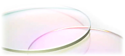
Photoresist Deposition for Microelectronics – Beyond Wafers
For large flat panels, large lenses, and curved or freeform optics where spin-coating is impractical, ultrasonic spray deposition lays down uniform photoresist films across full surfaces and over features, greatly reducing edge bead. This enables anti-reflective and diffractive structures and other lithography steps without pooling or streaking.
For microfluidic and biosensor substrates and roll-to-roll films or foils, spray-applied photoresist provides highly uniform, solvent-compatible thin films with superior adhesion and pattern fidelity. High transfer efficiency and closed-loop control minimize chemistry use while maintaining consistent dielectric and polymer layer thickness across each substrate.

CNTs, Nanowires, Conductive Inks & Nanomaterials
Sono-Tek’s ultrasonic nozzles deposit CNTs, nanowires, conductive inks, and other nanosuspensions as uniform, ultra-thin functional films on complex geometries. The ultrasonic vibrations of the atomizer create a natural deagglomerating effect—breaking apart clumps of nanoparticles that tend to form in suspension. This restores the particles to their original, independent nano-state, allowing them to perform as intended and maintain optimal electrical, optical, or mechanical properties.
By keeping particles evenly dispersed within the aerosol, the process prevents clogging, enhances coating uniformity, and ensures consistent conductivity and film performance. These coatings enable transparent conductors, heaters, EMI shields, antennas, and sensor layers, with precise control of coating materials and solvent delivery—scaling seamlessly from benchtop R&D to wide-format production.
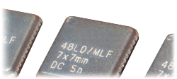
EMI Shielding
EMI shielding via ultrasonic spray is an emerging, high-potential approach that forms continuous, uniform conductive films on intricate packages and enclosures with precise thickness control. Many manufacturers are adopting spray deposition to replace or complement costlier methods like MOCVD or shield caps—reducing coating material use, assembly steps, and overall weight. Sono-Tek systems deliver consistent adhesion and conductivity for both polymer-based and metallic coatings, supporting the transition from R&D to in-line production.
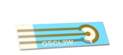
Sensors
For sensors and MEMS devices, ultrasonic spray enables the application of functional and protective coatings such as catalytic metal-oxide films, conductive or dielectric layers, enzyme or biorecognition materials, and hydrophobic or silicone-based overcoats. Low-velocity ultrasonic atomization protects sensitive structures while maintaining tight thickness and uniformity. These coatings enhance device durability, adhesion, and electrical performance from laboratory development to panel and roll-to-roll manufacturing.

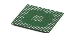
MicroLED / OLED / Advanced Displays
MicroLED display coating processes are primarily at the R&D and pilot-line stage today, with momentum building toward scalable thin-film encapsulation and precision flux deposition. In microLED assembly, one of the most critical steps is applying a thin, uniform layer of flux onto the backplane’s bonding pads before LED placement. This flux removes oxides, promotes wetting, and ensures strong solder adhesion during the subsequent reflow bonding process—directly impacting yield and long-term display reliability.
Sono-Tek’s ultrasonic spray technology provides the ideal solution for this step, delivering a micro-thin, perfectly uniform flux film across millions of tiny pads with exceptional repeatability. The low-velocity atomization and precise nozzle control eliminate splattering and excess residue, enabling clean, high-adhesion joints for each microLED-to-pad connection. By improving solder wetting uniformity and minimizing contamination, Sono-Tek systems have demonstrated measurable yield improvements—helping customers achieve production-level success where conventional methods struggle.
Beyond fluxing, Sono-Tek platforms also support polymer and organic coating materials used in thin-film encapsulation, planarization, and getter applications. Our technology allows manufacturers to refine coating solutions and solvent formulations efficiently, transferring validated recipes from development to pilot and early production with high material transfer efficiency and precise film control.
Flip-Chip Fluxing
For flip-chip fluxing, ultrasonic spray applies micro-thin, uniform flux films to bumps and pads, improving wetting and joint reliability during reflow while minimizing residue and splatter. The system’s closed-loop liquid delivery and precise nozzle control allow consistent flux volume, ensuring repeatability and preventing bridging or misalignment. This process scales smoothly from prototype development to in-line production for high-density PCB and semiconductor packaging applications.
Sono-Tek partners with global electronics manufacturers to deliver scalable, solvent-compatible, non-clogging ultrasonic spray coating systems for next-generation microelectronics. Our expertise spans polymers, silicones, and nanomaterial coatings—helping customers enhance adhesion, film uniformity, and dielectric performance across a wide range of electronic devices.